
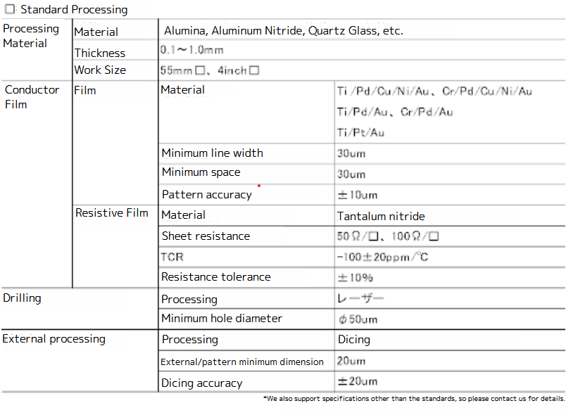
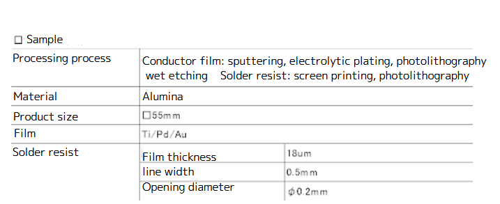
Thin film deposition system that combines film deposition technology using sputtering and vacuum evaporation with photo-etching technology, and a thick-film process using screen printing methods, and is capable of metallising, patterning and forming wiring of various metal films on ceramics and glass materials.
Various processed products, including ceramic substrates, are used in a wide range of fields to meet customer needs, such as space and defence applications, information and communications applications and industrial equipment applications.
Thin film deposition system
| Item(s) | Method | |||
| Process | Film deposition (sputtering +Film Deposition), Patterning (etching, lift-off, pattern plating) Laser cutting, dicing cutting, etc. |
|||
| Substrate Material |
Materials |
Alumina (96%, 99.6%), aluminium nitride,Fused quartz, ferrite, etc. Both in-house procurement and supplied base materials are possible, and base material polishing is possible. |
||
|
Thickness |
0.1-1.0 mmt approx. | Processing size | Up to Φ6inch or □4inch | |
| Film |
Conductor |
Ti/Pd/Au、Ti/Pd/Cu/Ni/Au、NiCr/Au、Ti/Pt/Au Cr/Pd/Au、Cr/Pd/Cu/Ni/Au |
||
| Resistor | Ta2N | Solder | AuSn | |
|
Solder Dams |
Cr、Solder mask | |||
|
Patterning |
Min. L/S |
30/30um | Dimensional Tolerances | ±0.01mm |
|
Through Hole |
Min. Diameter |
Φ50um | ||
|
Dicing |
External Tolerance<-Film process |
±0.05mm | ||
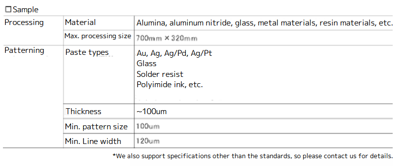
Thick-Film process
| Item(s) | Method | |||
| Process | Screen printing, etc. | |||
| Substrate Material | Materials | Alumina, glass, etc. Both in-house procurement and supplied base materials are possible. |
||
| Size | Up to approx. 720 x 320 mm | |||
| Patterning | Printing materials | Au、Ag、Ag/Pt、Ag/Pd、Glass, solder mask, polyimide, etc. | ||
| surface processing | Ni、Pd、Au (Plating) | Min. L/S | 100/120um | |
| Outline Cut | Cut Method | Scribe or dicing | Dimensional Tolerances | ±0.05mm~ |
Equipment
| Manufacturing Equipment | Sputtering Equipment, Evaporation equipment, Electrolytic Plating Baths, Exposure Equipment, Developers, Etching, Laser Processing Machines, Dicing Equipment, Screen Printing Machines, Various Ovens, Furnaces, etc. |
| Inspection Device | Scanning Electron Microscopes (SEM), CNC Image Measuring Instruments, Stereo-Microscopes, Laser Microscopes, Metallurgical Microscopes, Surface Roughness Meters, X-ray Fluorescence Film Thickness Meters, Multimeters, LCR Meters, etc. |
| Test Equipment | Constant Temperature Chambers, Ultra-low Temperature Chambers, Thermal Shock Chambers, Various Bonders, etc. |
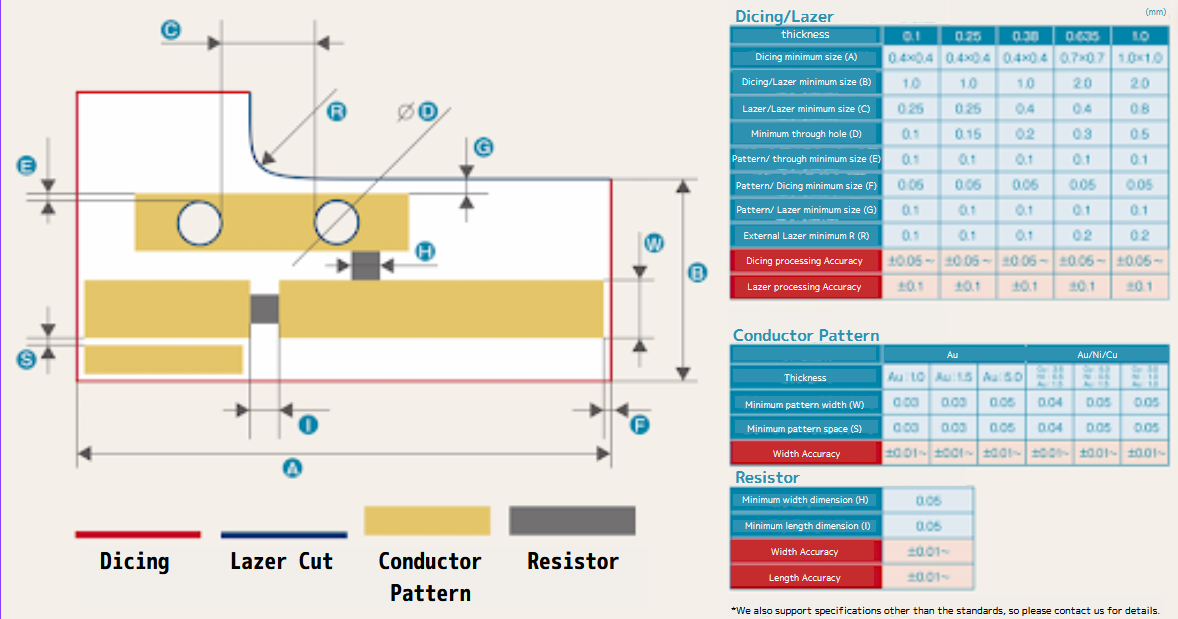
Standard design rules (thin-film processes)
Strengths
- Complex machining – Thin/thick film processes and a combination of internal and external resources enable a wide range of products to be processed.
- Ability to meet deadline – Proactively takes on the challenge of short delivery times on request, with a track record of 2-week turnaround times for new products
- Sales proposal capability – Timely proposal of optimum processes/processing methods to meet customer needs.
- Quality assurance – Quality assurance system, from various measurements to reliability tests, based on experience in supplying products to the space sector.
Latest News
- Introduction of evaporation equipment Start of supply of mass-produced products with Pt film specifications
- New CO₂ laser processing machine was introduced.
- Started operation of automatic trimming equipment.
Samples
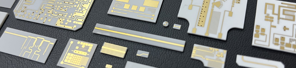
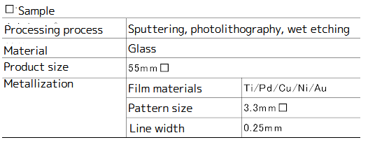
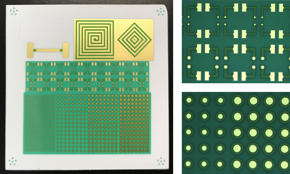
Sample1 Thin Film Circuit Substrate
Circuit boards based on vacuum deposition, photolithography and wet etching. Wide range of processing variations.
By selecting and combining the most suitable processing processes according to the required specifications from a wide range of processing variations, a high degree of design freedom can be achieved,
High-quality thin-film circuit boards can be supplied. We can also process supplied base materials and handle only certain processes.
Please feel free to contact us for more information.
 |
 |
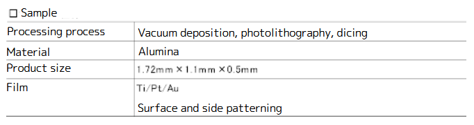
Sample2 Thin-film side metallised substrates
Due to the increasing demand for high-density mounting of multiple elements as devices become smaller and thinner,
Building patterning technology for the sides of substrates such as high heat dissipation ceramic substrates such as alumina and aluminium nitride.
Circuit formation can be carried out on one to four sides.
 |
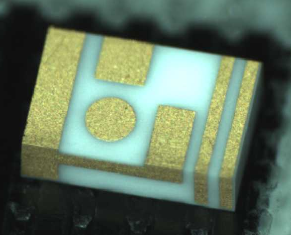 |
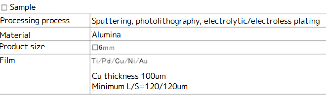
Sample3 Thin-film circuit boards with thick copper
Thick copper pattern formation on fine ceramic substrates to meet the needs of high current and high heat dissipation.
Copper electrode patterns with thicknesses of up to 100um can be formed with fine pitch using thin-film processes.
 |
 |
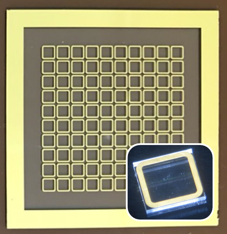
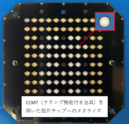
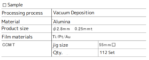
Sample4 Metallisation for metal bonding and sealing
Thin-film metallisation process for the periphery of glass lenses and sapphire caps.
Formation of metallised films for highly airtight and reliable metal bonding and sealing with packages and substrates.
By using our metal trays with clamping function “CCMT”, not limited to the above applications,
It can also be used for metallising individual chips.
  |
  |
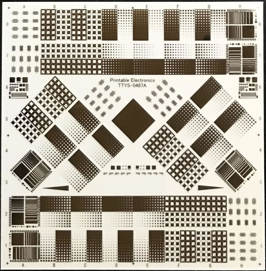
Sample5 Thick-film circuit boards
Circuit boards using screen printing methods. Based on past processing experience, the screens and pastes to be used are selected and the optimum specifications are proposed and products are processed according to requirements.
We select the screens and pastes to be used based on our past processing experience, propose the optimum specifications and process the product according to the customer’s requirements.
Compared with thin-film processes, the screen-printing method requires fewer labour costs and can be used in large lots at a lower cost, which is a feature of the screen-printing method.
Proudly introduce by us, please feel free to contact us for trial production.
 |
 |
Sample6 Circuit formation + Solder mask printing
Circuit boards with a solder mask pattern on the surface layer to prevent solder adhesion and ensure insulation reliability.
Fine resist patterns with stable film thickness can be formed by combining screen printing and photolithography.
Fine resist patterns can be formed with a stable film thickness by combining screen printing and photolithography. Solder mask printing alone is also available.
 |
 |